LCD Description
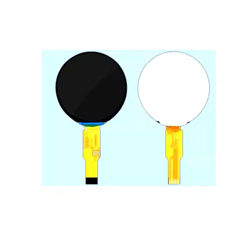
This circular LCD screen module 1.8 inch features a crystal-clear resolution of 360 * RGB * 360 pixels. Utilizing advanced IPS (In-Plane Switching) display technology, this circular LCD screen module 1.8 inch delivers stunning visual clarity and true-to-life color accuracy. Unlike standard TN screens, the premium IPS panel ensures ultra-wide, full viewing angles. This means your users can read critical data clearly from any perspective, whether they are glancing at a smartwatch during a workout or checking an industrial instrument in the field.
Engineered for seamless system integration, this high-performance circular LCD screen module 1.8 inch is powered by the highly efficient ST77916 driver IC. To optimize hardware design complexity, it utilizes a high-speed QSPI (Quad SPI) interface. The 4-wire QSPI protocol significantly reduces the required pin count on your microcontroller (MCU) or processor while maintaining blazing-fast data transmission speeds. This allows for smooth UI animations, quick screen refreshes, and reduced power consumption—making this circular LCD screen module 1.8 inch the ideal choice for battery-operated smartwatches, healthcare monitors, and compact IoT devices.
| Item | Contents | Unit |
| Size | 1.8 | inch |
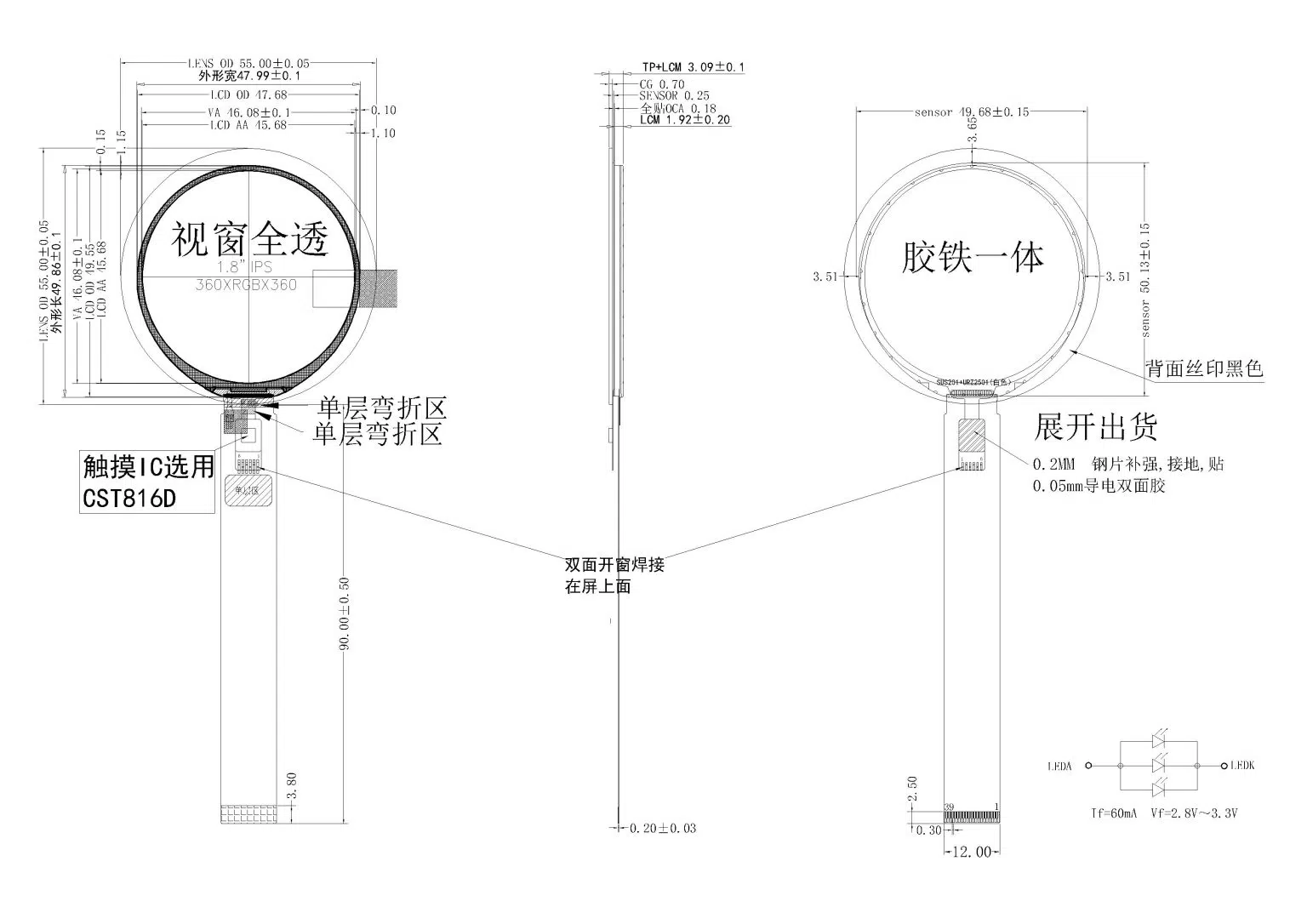
| LCM Dimension | 47.99(W)* 49.86(H) * 1.96(T) | mm |
| LCD Active Area | 45.68* 45.68 | mm |
| Number OfDots | 360* RGB * 360 | pixel |
| LCD Type | a-Si TFT | |
| Viewing Direction | ALL O’clock | |
| Driver IC | ST77916 | |
| Interface Type | MIPI/QSPI/8BIT/SRGB | |
| Operating Temperature | -20℃~ 70℃ | |
| Storage Temperature | -30℃~ 80℃ | |
| Backlight | 320 cd/m² | |
| Touchscreen | TBD |
Drawing
QSPI Interface
| NO | SYMBOL | FUNCTION | |||
| 1 | GND | Power Ground | |||
| 2 | LEDK | LED Cathode | |||
| 3 | LEDA | LED Anode | |||
| 4 | GND | Power Ground | |||
| 5 | CLKP | MIPI-DSI clock lane positive-end input pin | |||
| 6 | CLKN | MIPI-DSI clock lane negative-end input pin | |||
| 7 | GND | Power Ground | |||
| 8 | MIPI_D0P | MIPI-DSI data lane positive-end input pin. (Data lane 0 positive polarity)) | |||
| 9 | MIPI_D0N | MIPI-DSI data lane negative-end input pin.(Data lane 0 negative polarity) | |||
| 10 | GND | Power Ground | |||
| 11 | IM2 | IM1 | IMO | MPU Interface Mode | Data pin |
| IM1 | 0 | 0 | 0 | 3-line 9bit serial I/F | SDA: in/out |
| 0 | 0 | 1 | MIPI_3-line 9bit serial I/F | SDA: in/out DP/DN | |
| 12 | 0 | 1 | 0 | 2 data lane serial I/F | SDA1: in/out SDA2: in |
| IM2 | 0 | 1 | 1 | QSPI I/F | SDA[3:0]: in/out |
| 1 | 0 | 0 | RGB_3-line 9bit serial I/F | SDA: in/out DB[5:0]: out | |
| 13 | 1 | 0 | 1 | RGB_4-line 8bit serial I/F | SDA: in/out DB[5:0]: out |
| IM3 | 1 | 1 | 0 | 4-line 8bit serial I/F | SDA: in/out |
| 1 | 1 | 1 | 80-8bit parallel I/F | DB[7:0] | |
| 14 | IOVCC | Power Supply for logic, VDDIO=1.65V~3.3V. | |||
| 15 | VDD(3.3V) | Power Supply for Analog, VDD=2.4V~3.3V | |||
| 16 | VS | Vertical (Frame) synchronizing input signal in RGB interface | |||
| 17 | HS | Horizontal (Line) synchronizing input signal in RGB interface | |||
| 18 | TE | Tearing effect output pin to synchronize MCU to frame writing. This pin is low | |||
| when it is not activated. If not used, please open it | |||||
| 19 | RESET | This signal low will reset the device and must be applied to properly initialize the | |||
| chip. Signal is low active | |||||
| 20 | GND | Power Ground | |||
| 21 | D7 | Data signal for DBI Type B mode | |||
| 22 | D6 | Data signal for DBI Type B mode | |||
| 23 | D5 | Data signal for DBI Type B mode | |||
| 24 | D4 | Data signal for DBI Type B mode | |||
| 25 | D3(SDA3) | Data signal for DBI Type B mode | |||
| 26 | D2(SDA2) | Data signal for DBI Type B mode | |||
| 27 | D1(SDA1) | Data signal for DBI Type B mode | |||
| 28 | D0(SDA0) | Data signal for DBI Type B mode | |||
| 29 | CS | Chip select pin of DBI Type B mode. Low active. | |||
| 30 | RD(SCL) | Read Control pulse H duration | |||
| 31 | WR | Write enable in MCU parallel interface | |||
| 32 | DCX | Display data/command selection pin in parallel interface | |||
| 33 | GND | Power Ground | |||
| 34 | TP_SCL | TP clock | |||
| 35 | TP_SDA | TP data input | |||
| 36 | TP_RST | TP Reset pin | |||
| 37 | TP_INT | TP Communication interrupt for | |||
| 38 | TP_VCC | TP POWER SUPPLY | |||
| 39 | GND | Power Ground |