LCD Description
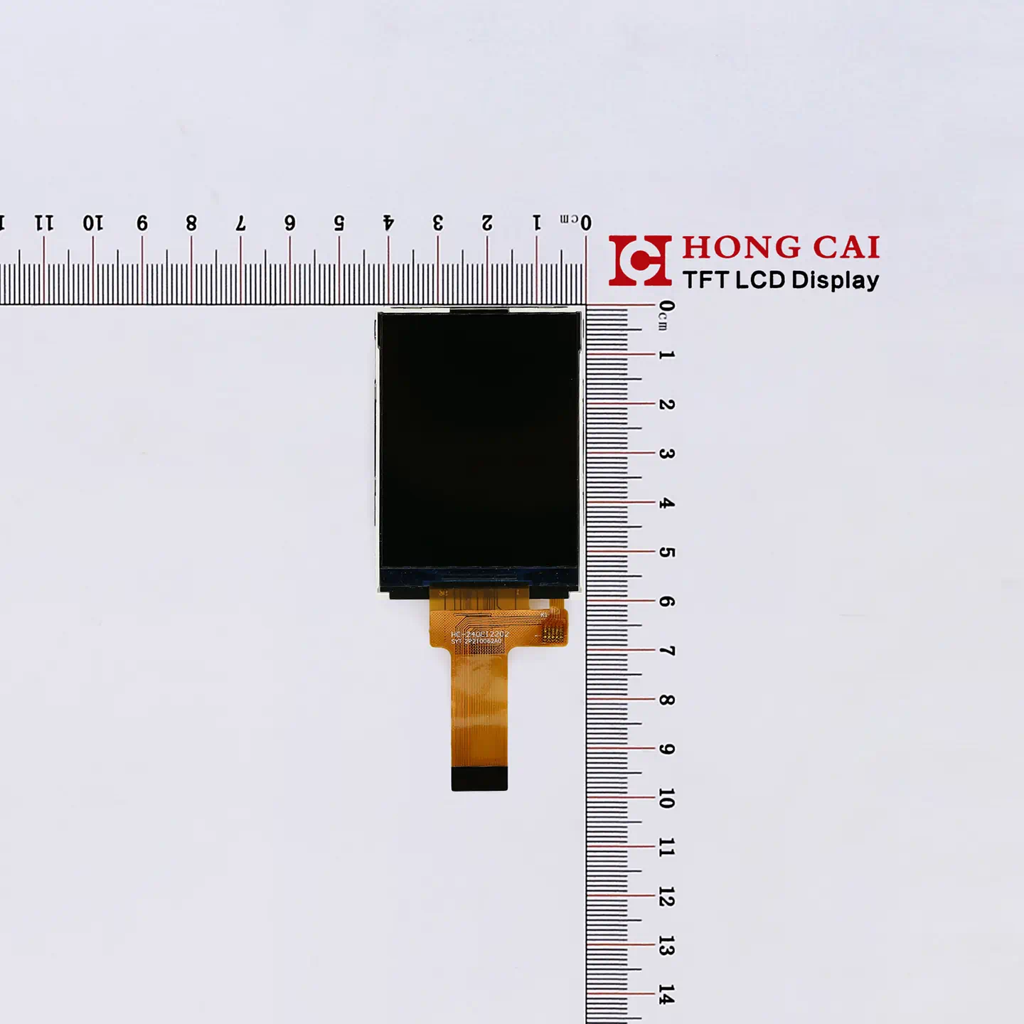
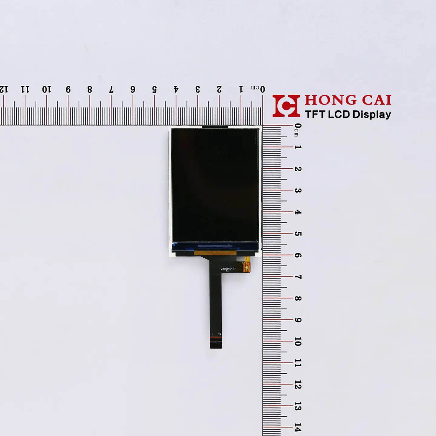
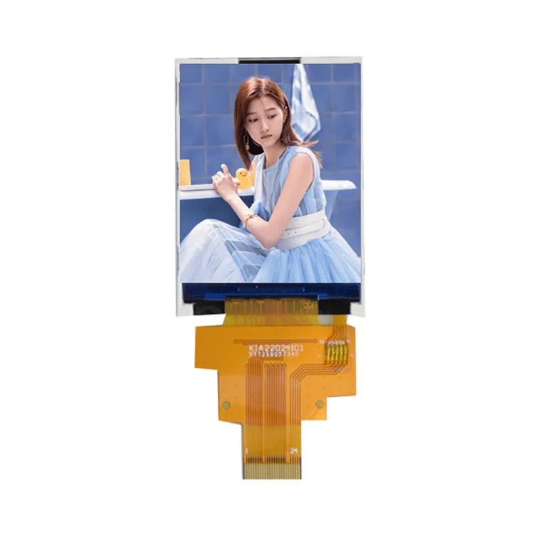
This premium TFT Display Screen 2.2 inch module is engineered to deliver exceptional visual clarity, vibrant colors, and dependable performance for next-generation smart hardware, handheld devices, and industrial equipment. Featuring a standard 240×320 dots resolution, this active-matrix liquid crystal screen utilizes optimized viewing technology to ensure a clear 12 O’clock viewing direction. As a highly versatile 2.2-inch TFT display, this unit is driven by the efficient ST7789V2 controller IC.
Operating via flexible interface options—including RGB, SPI, and MCU—this compact TFT display screen minimizes development complexity, allowing engineers to optimize power consumption and simplify hardware circuit design according to specific project requirements. If you are developing smaller handheld form factors, you can also check our SPI TFT LCD Display 2.0 inch series for layout comparison.
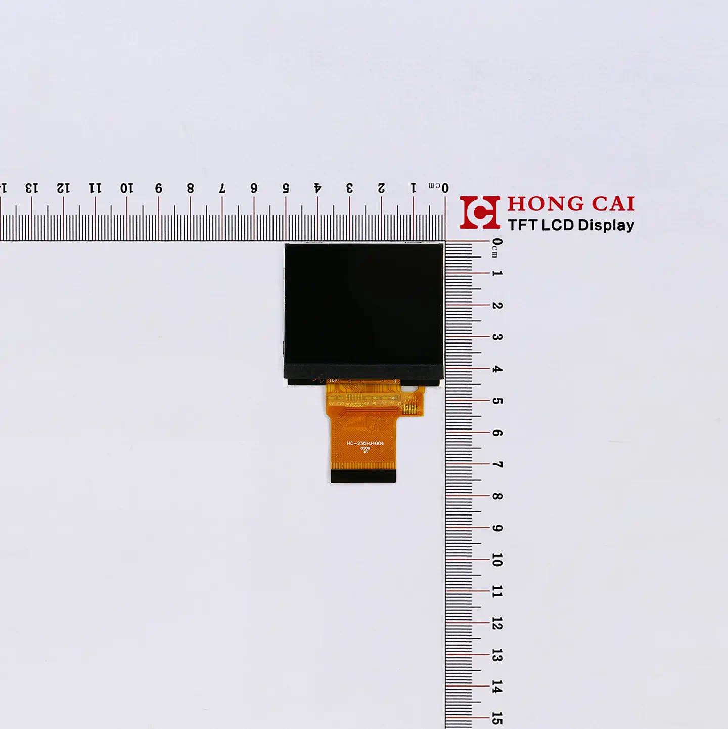
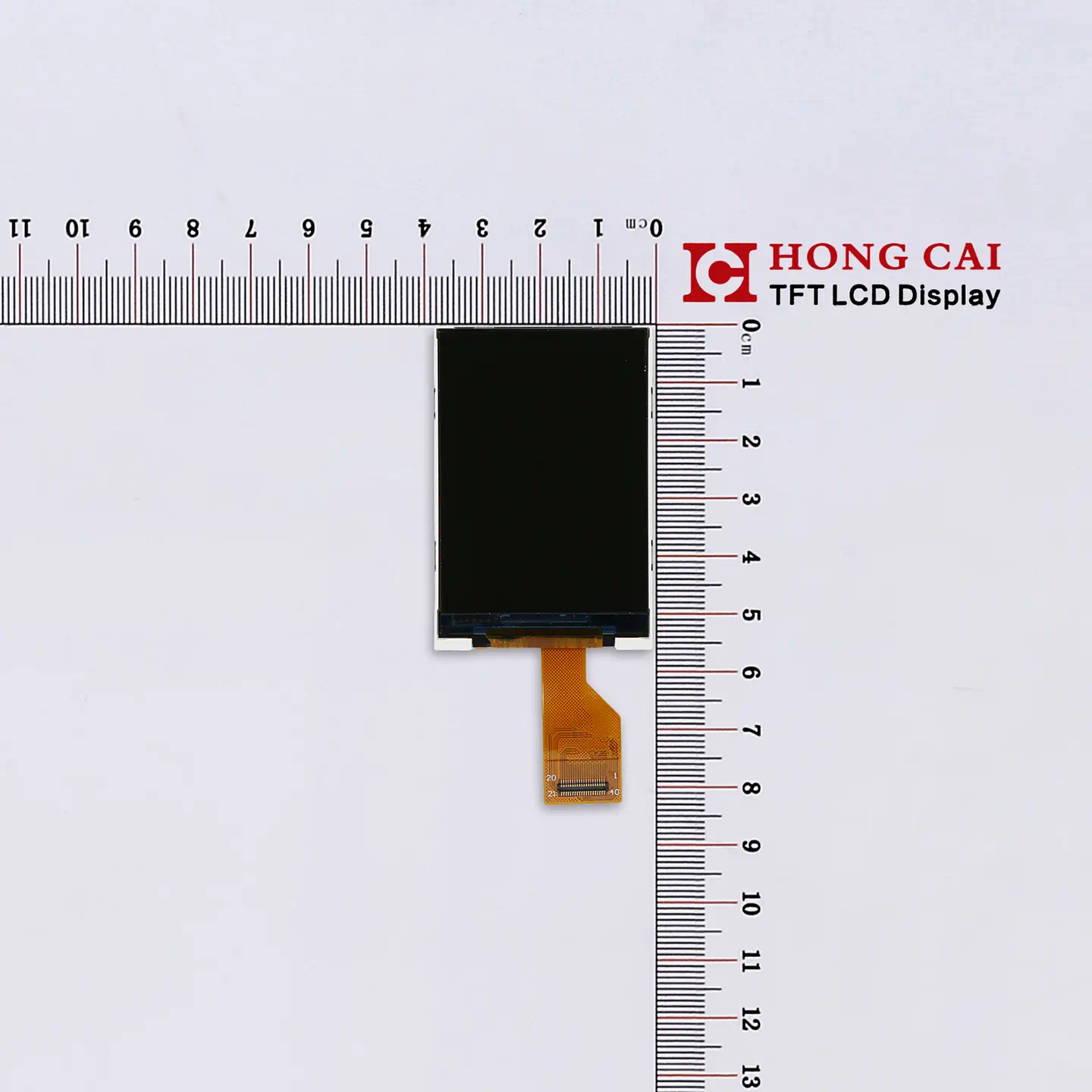
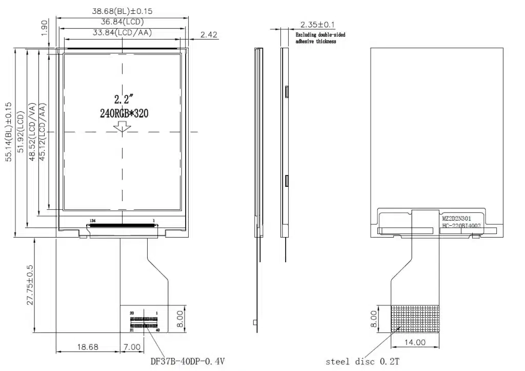
If your project requires a reliable, small-form-factor display with a precise outline dimension of 38.68 (W) * 55.14 (H) * 2.35 (T) mm, feel free to contact our engineering team for specialized factory-direct support.
| Item | Contents | Unit |
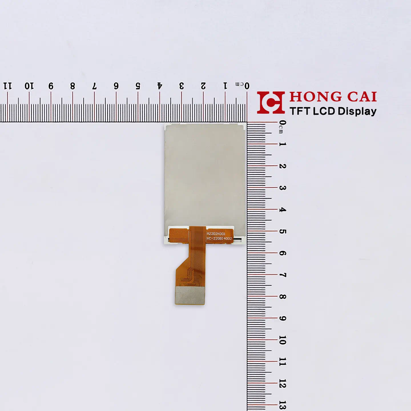
| Size | 2.2 | inch |
| LCM Dimension | 38.68(W)* 55.14(H) * 2.35(T) | mm |
| LCD Active Area | 33.84×45.12 | mm |
| Number Of Dots | 240×320 | pixel |
| LCD Type | a-Si TFT | |
| Viewing Direction | 12 O’clock | |
| Driver IC | ST7789V | |
| Interface Type | SPI/MCU/RGB | |
| Operating Temperature | -20℃~ 70℃ | |
| Storage Temperature | -30℃~ 80℃ | |
| Backlight | 320 | cd/m² |
| Touchscreen | TBD |
Drawing
RGB/SPI/MCU Interface
| NO. | Symbol | Description |
| 1-16 | DB15-DB0 | Data Bus |
| 17 | SDA | Serial Data Input |
| 18 | RD | Read signal, rising-edge-active. |
| 19 | WR | (MCU/ Write signal, rising-edge-trigger.) (SPI/Destination register selection.) |
| 20 | DC | (MCU Data/Command register address.)( SPI clock signal, rising-edge-trigger.) |
| 21 | CS | Chip Select |
| 22 | TE | Frame mark. |
| 23 | NC | NC |
| 24 | NC | NC |
| 25 | IOVCC | I/O POWER SUPPLY |
| 26 | VCC | POWER SUPPLY |
| 27 | GND | Ground |
| 28 | LEDA | BACKLIGHT ANODE |
| 29 | LEDK | BACKLIGHT CATHODE |
| 30 | LEDK1 | BACKLIGHT CATHODE |
| 31 | IM0 | Interface mode selection. |
| 32 | IM1 | Interface mode selection. |
| 33 | IM2 | Interface mode selection. |
| 34 | RESET | Reset pin |
| 35 | VS | Frame Synchronizing Signal |
| 36 | HS | Line Synchronizing Signal |
| 37 | PLCK | Dot Clock Signa |
| 38 | DE | Data Enable Signal |
| 39 | DB17 | Data Bus |
| 40 | DB16 | Data Bus |