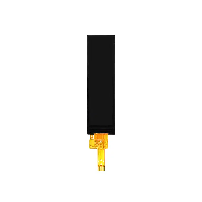
LCD Description
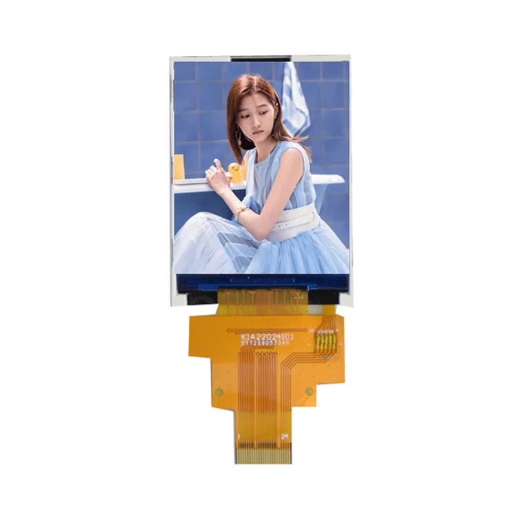
This premium 2.4 inch MCU TFT LCD display is engineered to deliver exceptional visual clarity and reliable performance for space-constrained embedded systems and HMI applications. Featuring a sharp 240×320 dots resolution and a responsive resistive touch screen, this compact color screen ensures user-friendly interaction, vibrant graphics, and consistent display quality with its solid 420 cd/m² backlight brightness.
As a leading factory in China, we ensure every MCU TFT LCD Display module undergoes rigorous quality control. This 2.4-inch variant utilizes an advanced MCU TFT LCD Display interface architecture, minimizing the standard I/O port requirement on your microcontrollers. If your project demands a reliable, compact, and high-brightness solution, this premium MCU TFT LCD Display with resistive touch integration is your ideal choice.
| Item | Contents | Unit |
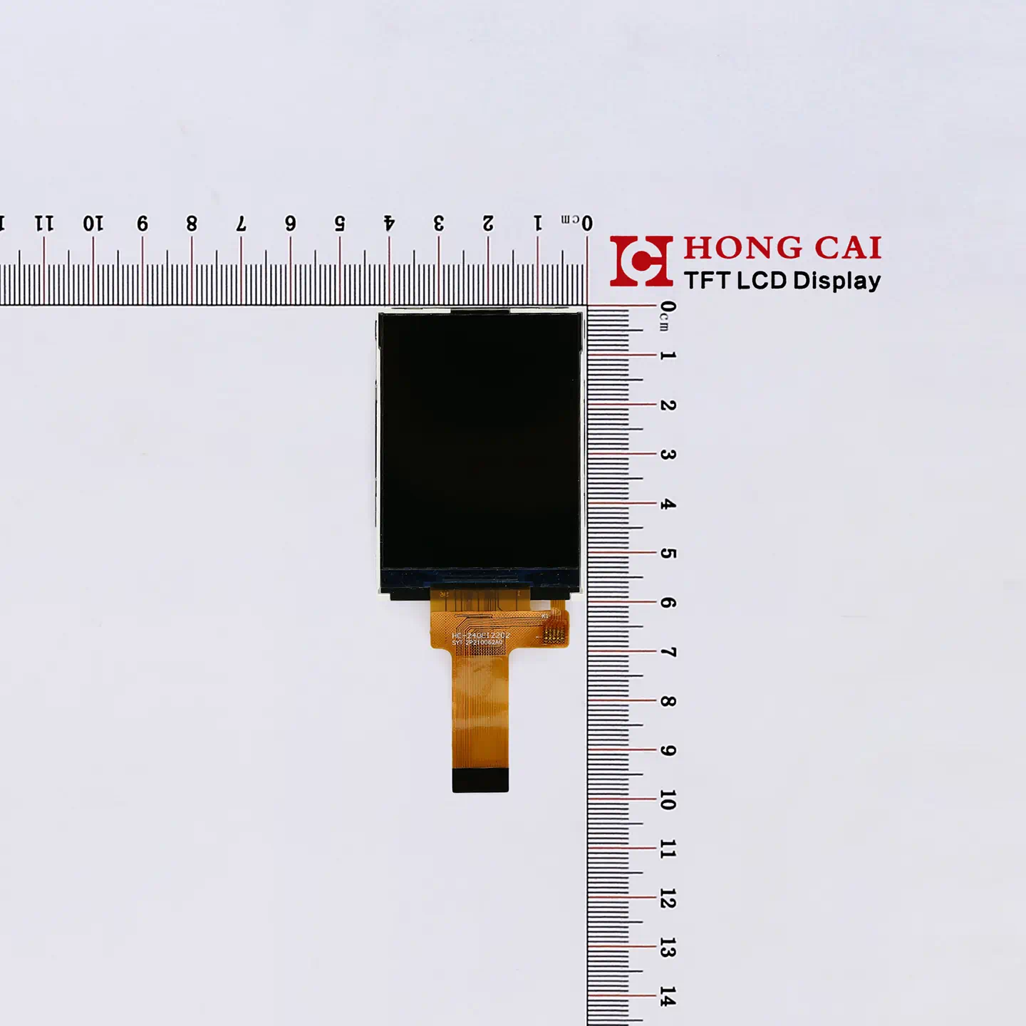
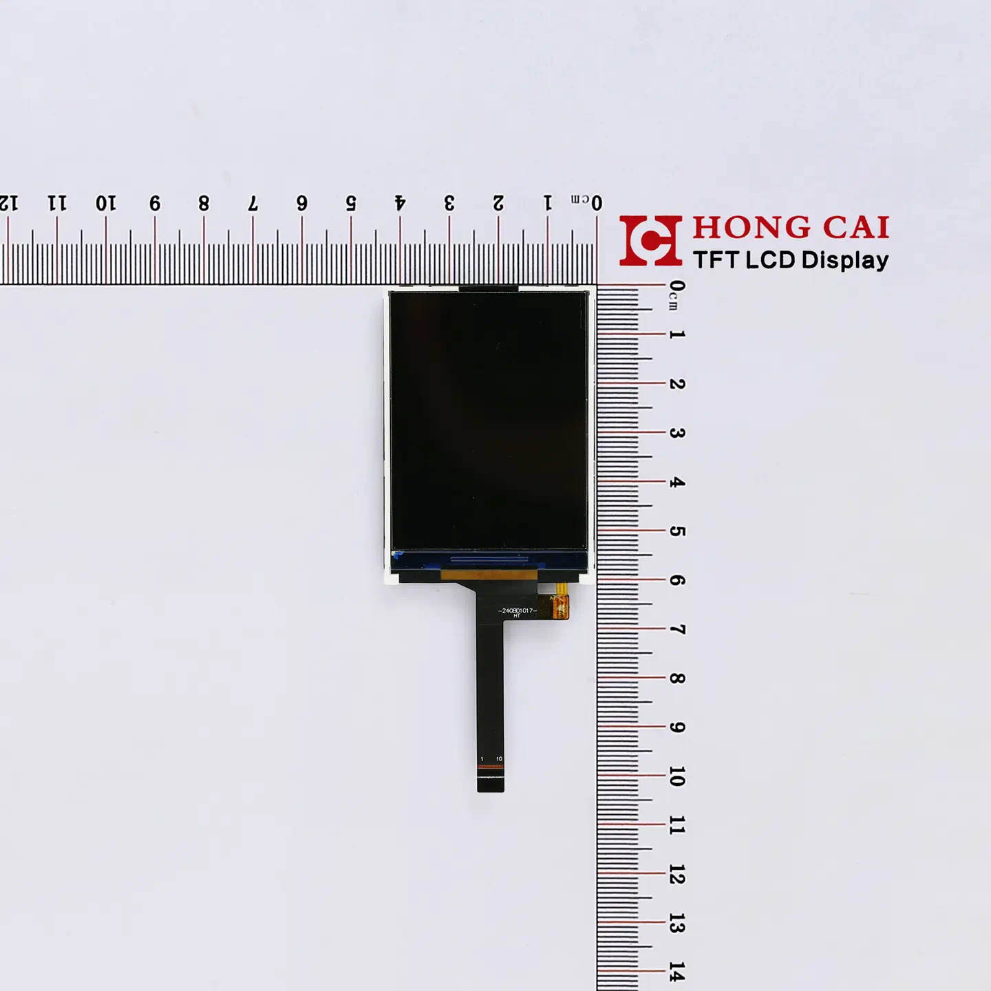
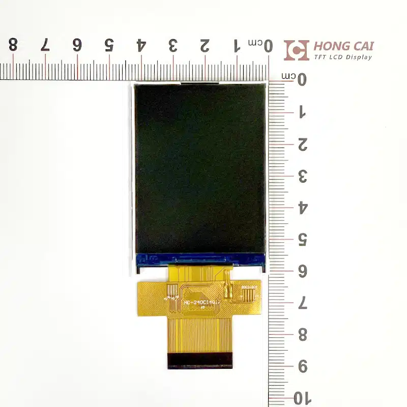
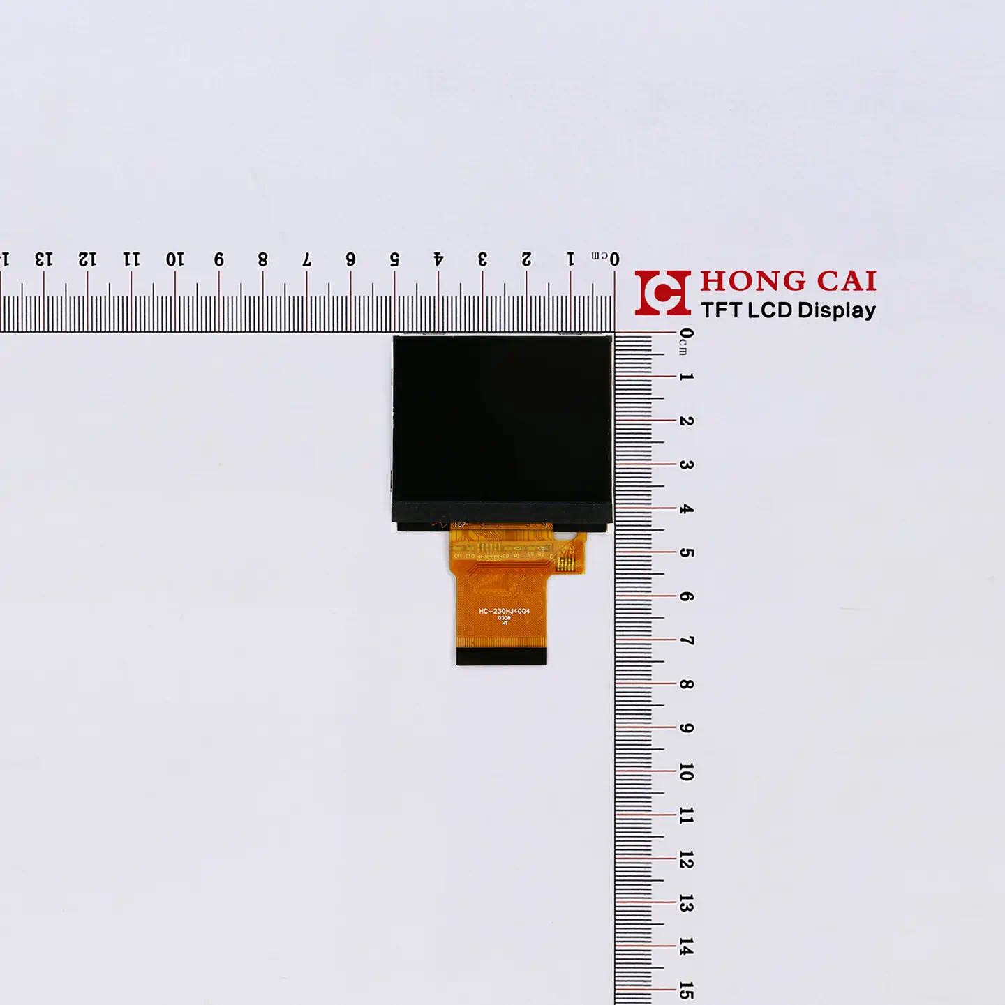
| Size | 2.4 | inch |
| LCM Dimension | 42.72(W)* 60.26(H) * 2.30(T) | mm |
| LCD Active Area | 36.72 × 48.96 | mm |
| Number OfDots | 240×320 | pixel |
| LCD Type | a-Si TFT | |
| Viewing Direction | 12 O’clock | |
| Driver IC | ST7789 | |
| Interface Type | MCU | |
| Operating Temperature | -20℃~ 70℃ | |
| Storage Temperature | -30℃~ 80℃ | |
| Backlight | 320 | cd/m² |
| Touchscreen | 电阻触摸屏 |
Drawing
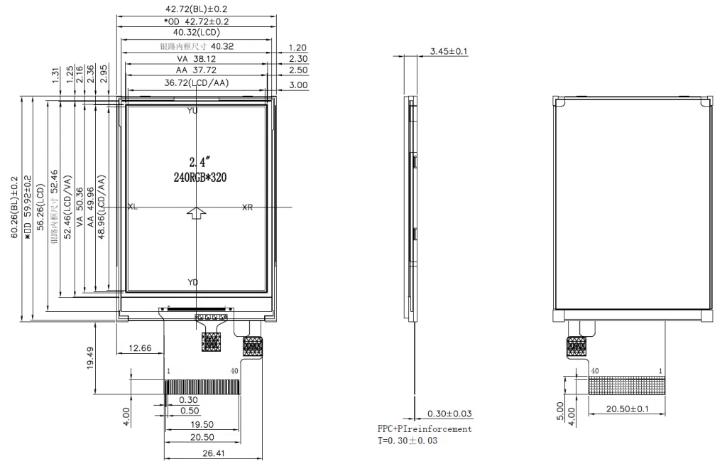
MCU Interface
| No. | Symbol | Function |
| 1 | GND | Ground |
| 2 | LEDA | Anode of backlight |
| 3-6 | LEDK1-LEDK4 | Cathode of backlight |
| 7 | XR | Touch panel X coordinate right |
| 8 | YU | Touch panel Y coordinate up |
| 9 | XL | Touch panel X coordinate left |
| 10 | YD | Touch panel Y coordinate down |
| 11 | RESET | Reset signal, keep Low for more than 10ms after power-on. |
| 12 | VHSYNC | DPI: Frame synchronizing signal Fix to DGND level when not in use. |
| 13 | HSHNC | DPI: Line synchronizing signal Fix to DGND level when not in use. |
| 14 | DOTCLK | DPI: Dot clock signal Fix to DGND level when not in use. |
| 15 | DEN | DPI: A data ENABLE input signal Fix to DGND level when not in use. |
| 16-21 | DB12-DB17 | Data bus |
| 22-27 | DB6-DB11 | Data bus |
| 28-33 | DB0-DB5 | Data bus |
| 34 | SDO | serial data output bi-direction pin Let it to open in MPU interface mode |
| 35 | SDI | DIN/SDA: serial data input/output bi-direction pin Fix to DGND level when not in use. |
| 36 | SCL | WRX pin, serves as a write signal SCL pin as Serial Clock when operates in the serial interface Fix to IOVCC level when not in use |
| 37 | CS | Chip select input signal Low: the chip is selected and accessible High: the chip is not selected and not accessible Fix to IOVCC level when not in use. |
| 38 | IOVCC | Connect to an external power supply of 1.65 ~ 3.3V. |
| 39 | VCI | Connect to an external power supply of 2.5 ~ 3.3V. |
| 40 | GND | Ground |