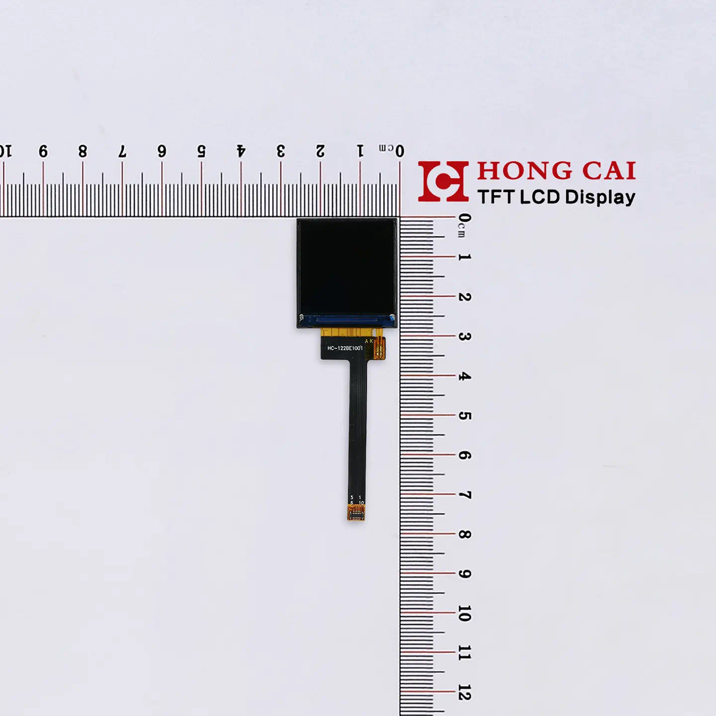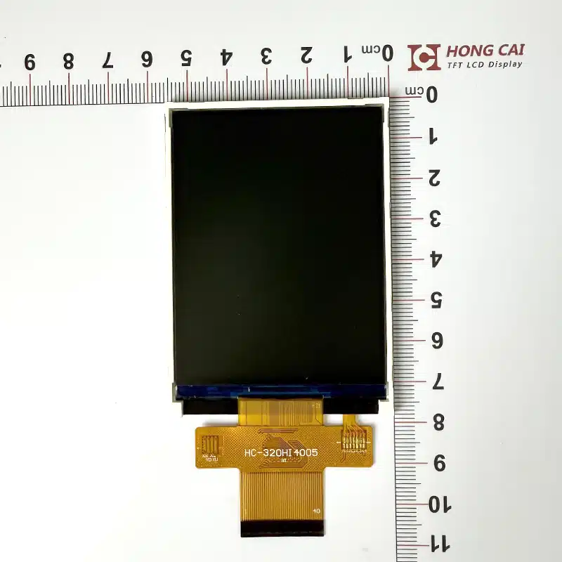
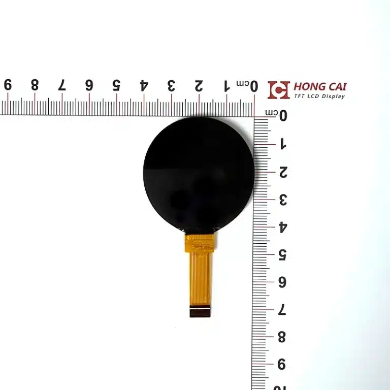
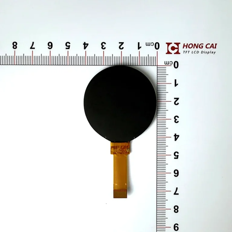
LCD Description
High-resolution 1.53″ Round LCD Display (360×360) featuring IPS technology for all-round viewing. Powered by ST77916 driver with QSPI interface. 320 cd/m² brightness and ultra-slim 2.14mm design. Ideal for smartwatches and wearable IoT devices.
| Item | Contents | Unit |
| Size | 1.53 | inch |
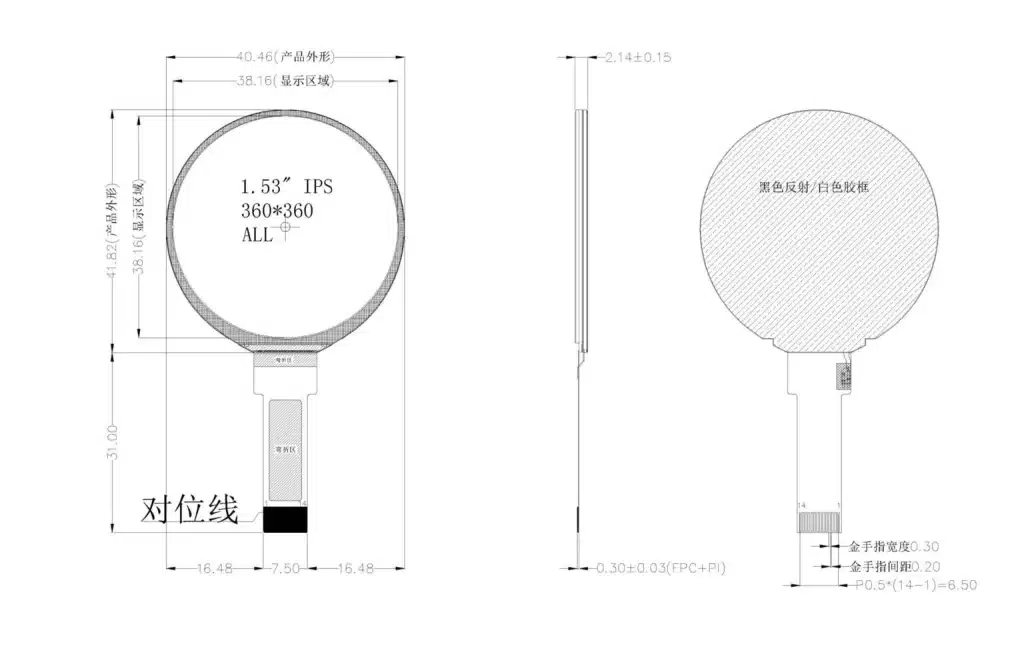
| LCM Dimension | 39.3×40.96×1.6 | mm |
| LCD Active Area | 37.3×37.3 | mm |
| Number OfDots | 360×360 | pixel |
| LCD Type | a-Si TFT | |
| Viewing Direction | ALL O’clock | |
| Driver IC | ST77916 | |
| Interface Type | QSPI | |
| Operating Temperature | -20℃~ 70℃ | |
| Storage Temperature | -30℃~ 80℃ | |
| Backlight | 320 | cd/m² |
| Touchscreen | TBD |
Drawing
SPI Interface
| Pin No. | Pin Name | Description |
| 1 | LEDK | Backlight cathode (negative) supply pin. Can be grounded via a current-limiting resistor if control is not required. |
| 2 | LEDA | Backlight anode (positive) supply pin. Voltage range: 2.9–3.1V (Typical: 3.0V). |
| 3 | GND | Display ground pin. |
| 4 | VDDIO | Power supply for display I/O interface (1.8–3.3V). |
| 5 | VDD | Power supply for display logic (2.8–3.3V). |
| 6 | TE | Tearing Effect (Frame sync signal). Used for camera synchronization; leave floating if not used. |
| 7 | RST | Display reset pin, active low. |
| 8 | D3 | QSPI serial data input channel 3. |
| 9 | D2 | QSPI serial data input channel 2. |
| 10 | D1 | QSPI serial data input channel 1. |
| 11 | D0 | QSPI serial data input/output channel 0. |
| 12 | CS | Chip Select pin for the display driver IC, active low. |
| 13 | SCL | QSPI serial clock signal (Max frequency: 50MHz). |
| 14 | GND | Display ground pin. |